Flexible low-voltage high-frequency organic thin-film transistors
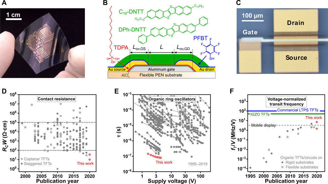
by Thamarasee Jeewandara, Tech XploreElectronic applications on unconventional substrates that require low-temperature processing methods have primarily driven the development of organic thin-film transistors (TFTs) in the past few decades. Such applications primarily require high-frequency switching (rate at which an electronic switch performs its function) or amplification at low operating voltages. However, most organic-TFT technologies show limited dynamic performance unless researchers apply high operating voltages to overcome their high contact resistances and large parasitic capacitances, i.e. a capacitance that exists between parts of electronic components or a circuit due to their proximity to each other. In this work, James W. Borchert and a team of interdisciplinary researchers in nanoscience, chemistry, quantum science and solid state research in Germany and Italy, presented low-voltage organic TFTs. The devices recorded static and dynamic performances including contact resistances as small as 10 Ω·cm, on/off current ratios as large as 1010 and transit frequencies as high as 21 MHz. The inverted coplanar TFT structure developed in this work can be readily adapted to industry-standard lithographic techniques.
Flexible electronics are presently a $20-billion-per-year industry driven by recent trends of active-matrix organic light-emitting diode (AMOLED) smartphone displays on polyimide substrates. Among the many challenges associated with the transition, scientists must reduce the process of the thin-film transistor (TFT) technology via low temperature polycrystalline silicon (LTPS), to make it compatible with polyimide substrates, while retaining the characteristics of TFT. In this work, Borchert et al. showed the capabilities of a previously reported method to develop low-voltage organic TFTs with low contact resistance for enhanced static and dynamic performance.
They fabricated the TFTs and circuits on flexible polyethylene naphthalate (PEN) sheets with high-resolution silicon stencil marks to pattern all device layers. The team combined the low contact resistance with a small channel length and small gate-to-contact overlaps to obtain record static and dynamic performances. They measured the dynamic performances of individual TFTs operating in the saturation regime using a two-port network analysis (an electrical network with two terminals connected to external circuits). Borchert et al. then measured the channel-length dependence of the transit frequency and determined a width-normalized contact resistance of 10 ± 2 Ω·cm. The experimental characteristics represented important proof-of-concepts to develop low-power flexible circuits based on organic TFTs for use in flexible AMOLED displays.
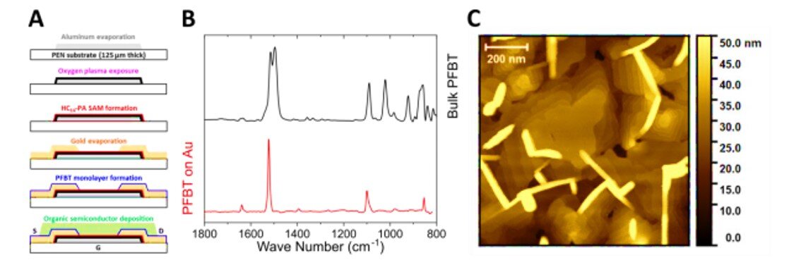
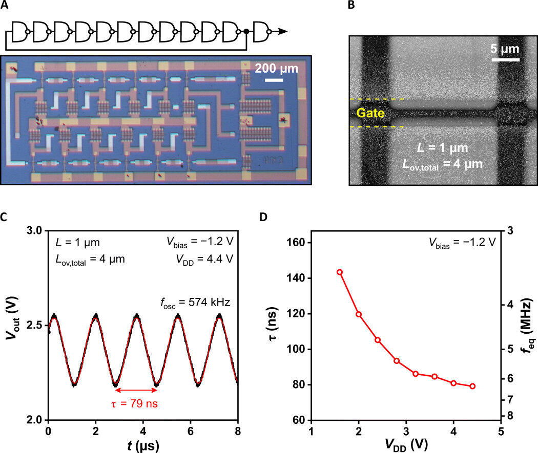
The team engineered small molecule organic semiconductors as the active layer of TFTs, on flexible polymer substrates with a channel length of 8 µm, a gate-to-contact overlap of 4 µm and a channel width of 200 µm. They determined the transfer and output characteristics of TFTs based on diverse semiconductors that constituted the device. The experimental results were similar to previous studies and confirmed good reproducibility of the fabrication process. During the experiments, the scientists used two types of semiconductor materials abbreviated DPh-DNTT and C10-DNTT to form thermally stable thin film transistors (TFTs). They then observed the static and dynamic circuit characteristics using an inverter composed of DPh-DNTT based TFTs and an 11-stage ring oscillator based on C10-DNTT based TFTs. The dimensions were identical in both circuits and maintained a similar biased-load design.
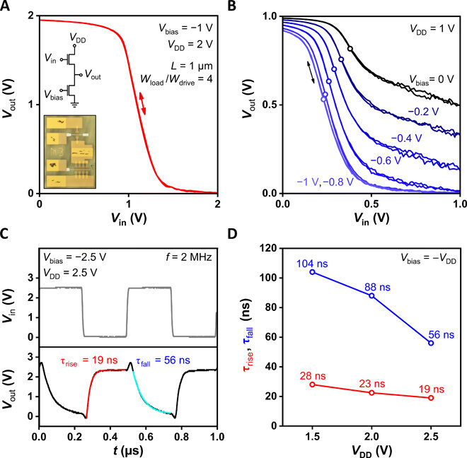
To understand the dynamic performance of the inverter, Borchert et al. applied a square-wave input signal with a frequency of 2 MHz and an amplitude of 1.5, 2.0 or 2.5 V. They detected the smallest time constants (19 and 56 nanoseconds—ns) for a supply voltage of 2.5 V and then summarized the results from the 11-stage ring oscillator. The team photographed the 11-stage ring oscillator circuit using scanning electron microscopy and measured its output signal. The signal-propagation delay in the setup was the smallest value reported to date (143 ns for a supply voltage of 1.6 V and 79 ns for a supply voltage of 4.4 V) at a supply voltage less than 50 V.
The team obtained more detailed information of the dynamic properties of individual TFTs using a two-port network analysis. Using scattering-parameter (S-parameter) measurements the team studied the high-frequency characteristics of organic TFTs. Based on the method, they performed detailed dynamic characterizations of thin film transistors and observed the area-normalized gate-drain capacitance to be constant with the frequency in all measurements. The scientists determined the transit frequencies and noted their dependence on the channel length to thereby extract the contact resistance and intrinsic channel mobility.
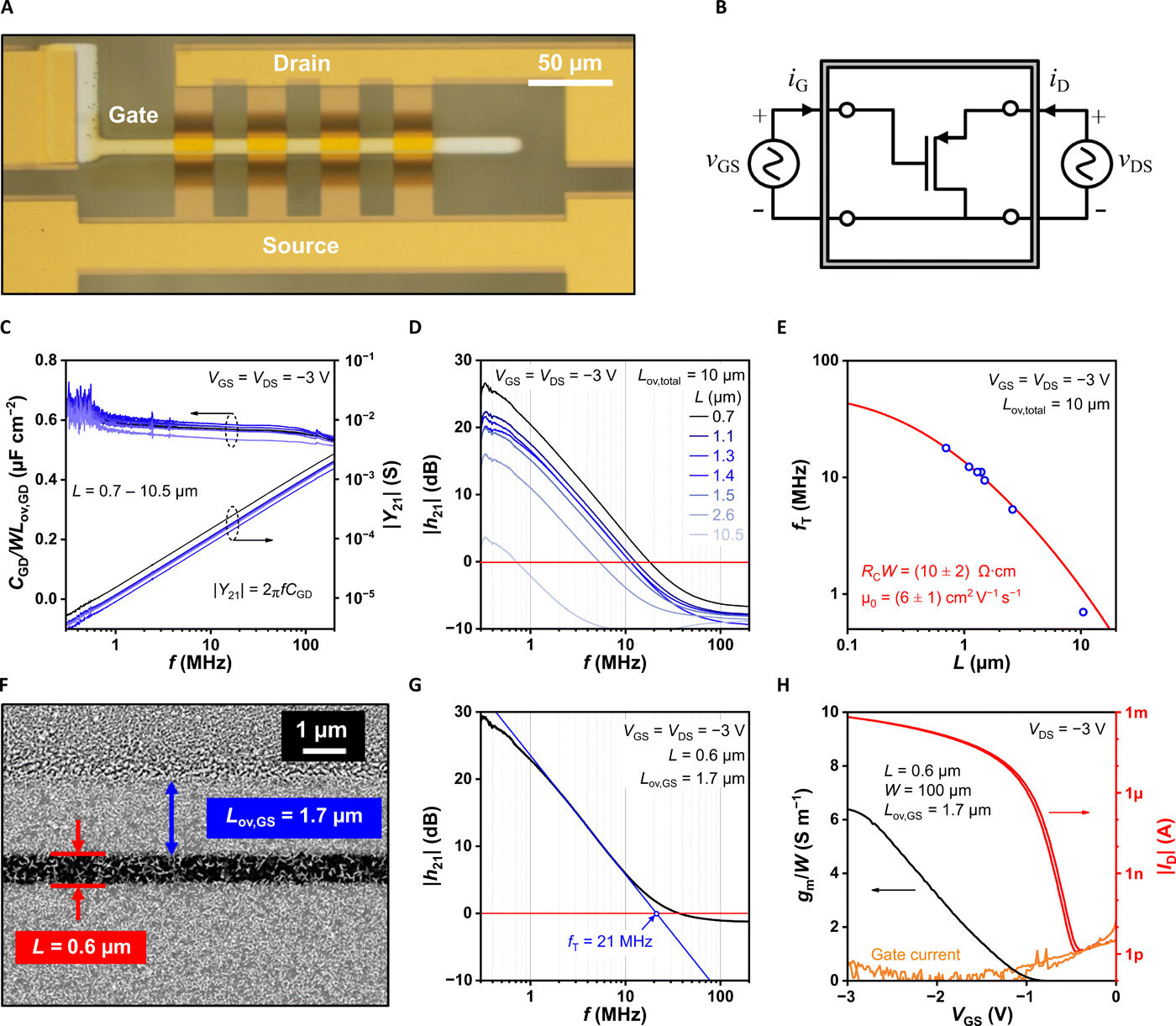
Parasitic fringe capacitance effects in the field-effect transistors could also arise when the semiconductor layer extended beyond the edges of the device. The team therefore reduced the gate-to-source overlap, while maintaining the total gate-to-contact overlap and the channel length constant to obtain a smaller total gate capacitance and a higher transit frequency. By optimizing the dimensions of the TFT, the scientists obtained a transit frequency of 21 MHz as the highest value reported to date for an organic transistor made on a flexible substrate. The results demonstrated the possibility of building organic TFTs on flexible substrates with static and dynamic performance for high-frequency mobile electronic applications. The results of the work approached those of industry-standard low temperature polycrystalline silicon TFTs, while using a TFT architecture that complied with existing industry-standard fabrication processes.
| More information: James W. Borchert et al. Flexible low-voltage high-frequency organic thin-film transistors, Science Advances (2020). DOI: 10.1126/sciadv.aaz5156 Kris Myny. The development of flexible integrated circuits based on thin-film transistors, Nature Electronics (2017). DOI: 10.1038/s41928-017-0008-6 Xinge Yu et al. Metal oxides for optoelectronic applications, Nature Materials (2016). DOI: 10.1038/nmat4599 Journal information: Science Advances , Nature Electronics , Nature Materials |