Calculate an R-C snubber in seven steps
by Steve BushPrompted by wise commenter of this parish Steve Kurt, I came across an excellent on-line app note by Texas Instruments about a step-by-step route to effectively snub voltage ringing at buck converter switch nodes.

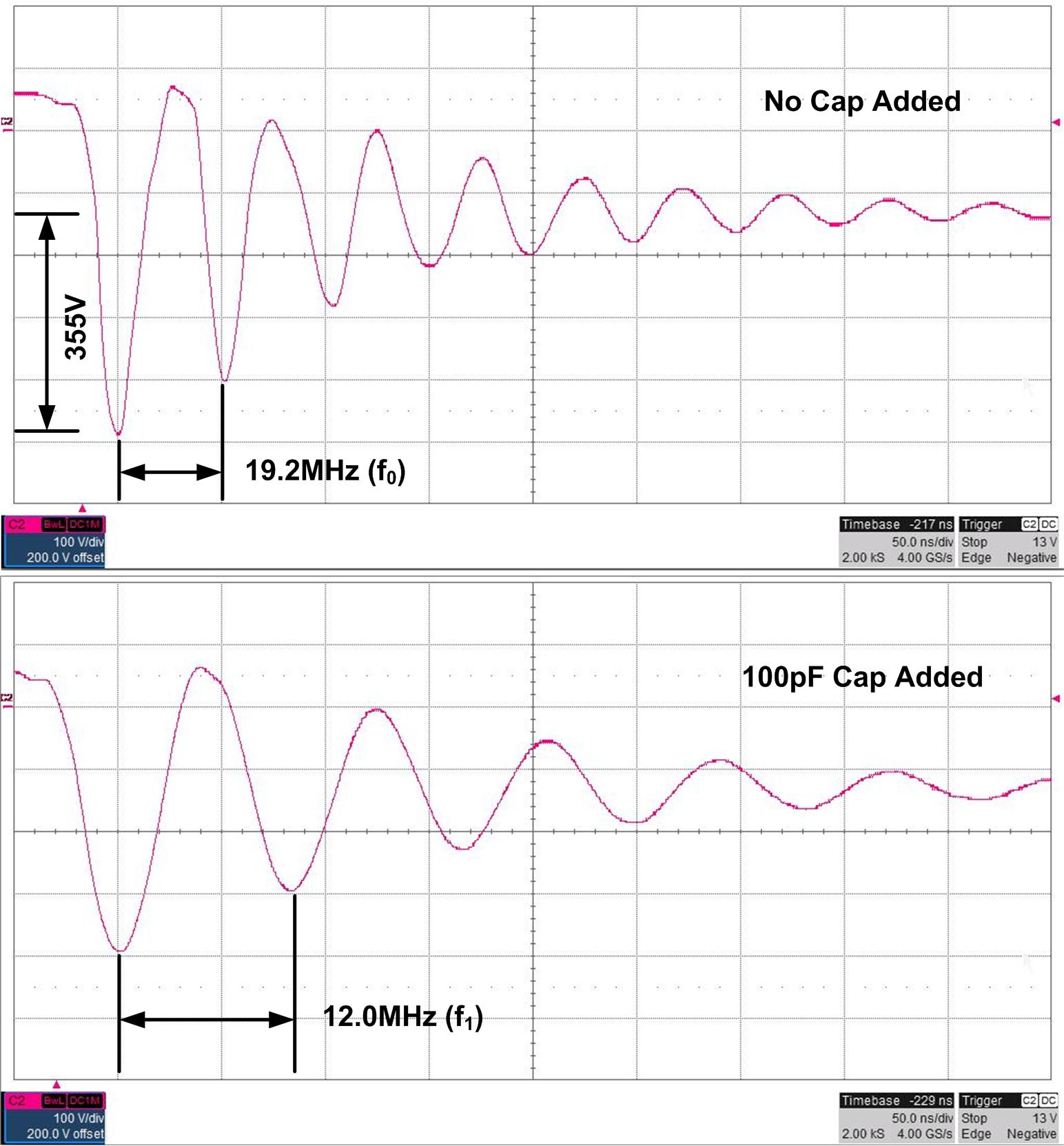
This ringing occurs after the power transistor is switched off, and is the result of residual energy, stray inductance and stray capacitance.
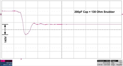
Although very noticeable on a scope (probe carefully, avoid long probe earth), the ringing does not actually harm circuit operation unless it is of such high voltage that it damages something. Snubbing it actually wastes power, but also removes a potentially strong source of EMI.

Anyway, the TI app note covers a straightforward 7 step process to a properly damped waveform
Hats off to TI,
and thanks to Mr Kurt.