Japan’s Hottest Stock Is Tiny Maker of $40 Million Machines
by Pavel Alpeyev, Kazu Hirano- Up About 550% since start of 2019, Lasertec is key supplier
- Company sells semiconductor testing machines to Samsung, TSMC
The list of Intel Corp.’s annual supplier award winners tends to read like a who’s-who of the semiconductor industry’s biggest names. This year, it included a little-known Japanese company whose machines have become indispensable in the race to improve semiconductors and whose stock has been rocketing up as a result.
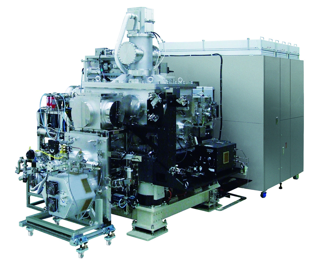
Lasertec Corp. is the world’s only maker of testing machines required to verify chip designs for the nascent extreme ultraviolet lithography (or EUV) method of chipmaking. In 2017, Lasertec solved a key piece of the EUV puzzle when it created a machine that can inspect blank EUV masks for internal flaws. Last September, it cleared another milestone by unveiling equipment that can do the same for stencils with chip designs already printed on them. This March, Intel gave the tiny Yokohama-based company an award for innovation, its first after decades of doing business together.
“That’s a major milestone for us,” Lasertec President Osamu Okabayashi said in an interview. “It means a lot to be recognized this way as a supplier.”

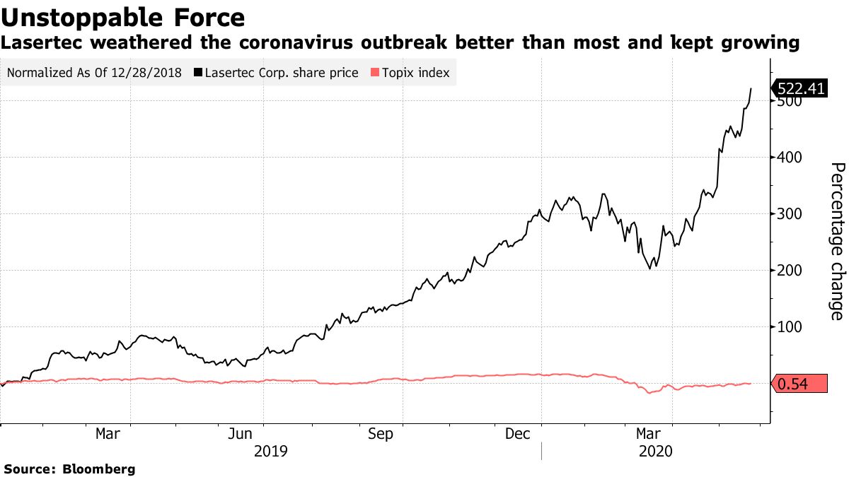
The company’s stock has soared about 550% since the start of 2019, more than twice the gain of the second-best-performing security in the benchmark Topix index. Shares increased about 4% Tuesday, pushing its rise this year to more than 60%.
Intel declined to say if it was buying EUV equipment from Lasertec, which already supplies test gear to its rivals Samsung Electronics Co. and Taiwan Semiconductor Manufacturing Co. The three chip fabricators are the only ones so far to announce EUV plans, because the technology is so complex and expensive. Okabayashi would only say that his company has “two or more” EUV customers.
“This can be read as a sign that Lasertec’s tools are indispensable to Intel’s EUV roadmap.” said Damian Thong, an analyst at Macquarie Group Ltd.

Read more: Japan’s Star Electronics Stock Will Be Vital to Intel, Samsung
EUV is just entering the mass production phase after two decades in development, but investors are already betting Lasertec will be one of the key beneficiaries. The move to EUV overcomes key hurdles to shrinking manufacturing geometries of semiconductors, allowing more and smaller transistors to be crammed onto silicon. It promises to unleash another wave of gadgets that are slimmer, cheaper and more powerful.
Last month, Lasertec raised its annual order forecast for the second time this year to 85 billion yen ($789 million) in the period ending June, nearly double the amount it received in fiscal 2019. The company is headed for the fourth straight year of record revenue and profits. Sales will climb 39% to 40 billion yen and profit will jump 76%, according to its estimates. And that’s likely to be just the beginning.
Samsung earlier this month said it is building a 5-nanometer fabrication facility that will use EUV to make processors for applications ranging from 5G networking to high-performance computing from the second half of next year. Taiwan’s TSMC is pushing ahead with plans to adopt 3-nanometer lithography mass production in 2022 and announced plans to build an advanced fab in the U.S. Intel’s first product made using EUV is expected late next year.
Their primary focus is on so-called logic processors, used to power devices and networking applications, but the new manufacturing technique will eventually filter through into the production of DRAM and other memory chips.
Read more: Samsung Takes Another Step in $116 Billion Plan to Take on TSMC
“Logic makers will be first to adopt EUV, with memory makers following later,” Okabayashi said. “The real volume of orders will come when they reach mass production stage. Right now it’s 7- and 5-nanometer chips. 3-nanometer is still in development stage.”
Okabayashi expects each customer will probably need several of his testers, which could cost well over $40 million apiece and take as long as two years to build. A chipmaker would need at least one machine in its mask shop to make sure the stencils come out right. Another would go into a wafer fab to keep an eye on the microscopic wear and tear that result from concentrated light being projected repeatedly through the chip design stencils.
“Lasertec is still trying to get a feel for this market and how big it can be,” Macquarie’s Thong said. “Their stock is moving on expectation of future orders. But there is little actual visibility on the scale of this market, so Lasertec retains a lot of capacity for surprise.”
— With assistance by Yuki Furukawa
(Updates with share price in fourth paragraph)