Process to produce well-aligned CNT arrays on a 10-centimeter silicon wafer
by Bob Yirka
A team of researchers affiliated with several institutions in China has developed a new process to produce well-aligned carbon nanotube (CNT) arrays on a 10-centimeter silicon wafer. In their paper published in the journal Science, the group describes their process and how well it compared to similar type silicon designs.
Scientists have known for many years that there would come a day when silicon processors would reach physical limits, as they can only be made so small. Because of that, scientists have been searching for a viable replacement. In this new effort, the researchers in China have been investigating the possibility of using CNT arrays as a replacement for silicon.
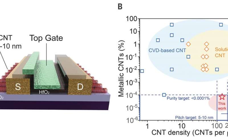
Carbon nanotubes are essentially one-atom-thick sheets of carbon rolled into tubes. They present the possibility of use in computer chips because they can be made to behave as semiconductors. Prior efforts have shown that individual CNTs can be used to create transistors, but a better approach is to use aligned groups of them. Impeding such research has been the challenge of producing CNTs that have the degree of consistency that is needed for such a precise application. Another challenge has been preventing the CNTs from turning metallic during processing. In this new effort, the researchers have produced well-aligned CNT arrays with higher consistency than other methods—and report that just one in a million turn out metallic.
The process involved putting CNTs in a toluene solvent and then adding a polymer to coat them. Next, the CNTs were run twice through a centrifuge that sorted them by semiconducting ability. The next step involved putting the CNTs into a liquid solution (along with a small amount of 2-butene-1,4-diol) and then dipping a silicon wafer into the solution. The butene diol in the solution coated the wafer while the CNTs formed hydrogen bonds. When the wafer was lifted from the solution, the CNTs self-assembled along the line that had formed between the butene diol and the wafer. The finished result was an array of aligned CNTs on a silicon wafer.
The method allowed for a density of between 100 and 200 per micrometer, up significantly from the 47 seen in other methods. The team also tested their process by using their CNT-covered silicon wafer to build a field-effect transistor, which they noted outperformed a similar transistor built using silicon.
More information: Lijun Liu et al. Aligned, high-density semiconducting carbon nanotube arrays for high-performance electronics, Science (2020). DOI: 10.1126/science.aba5980
Journal information: Science
© 2020 Science X Network