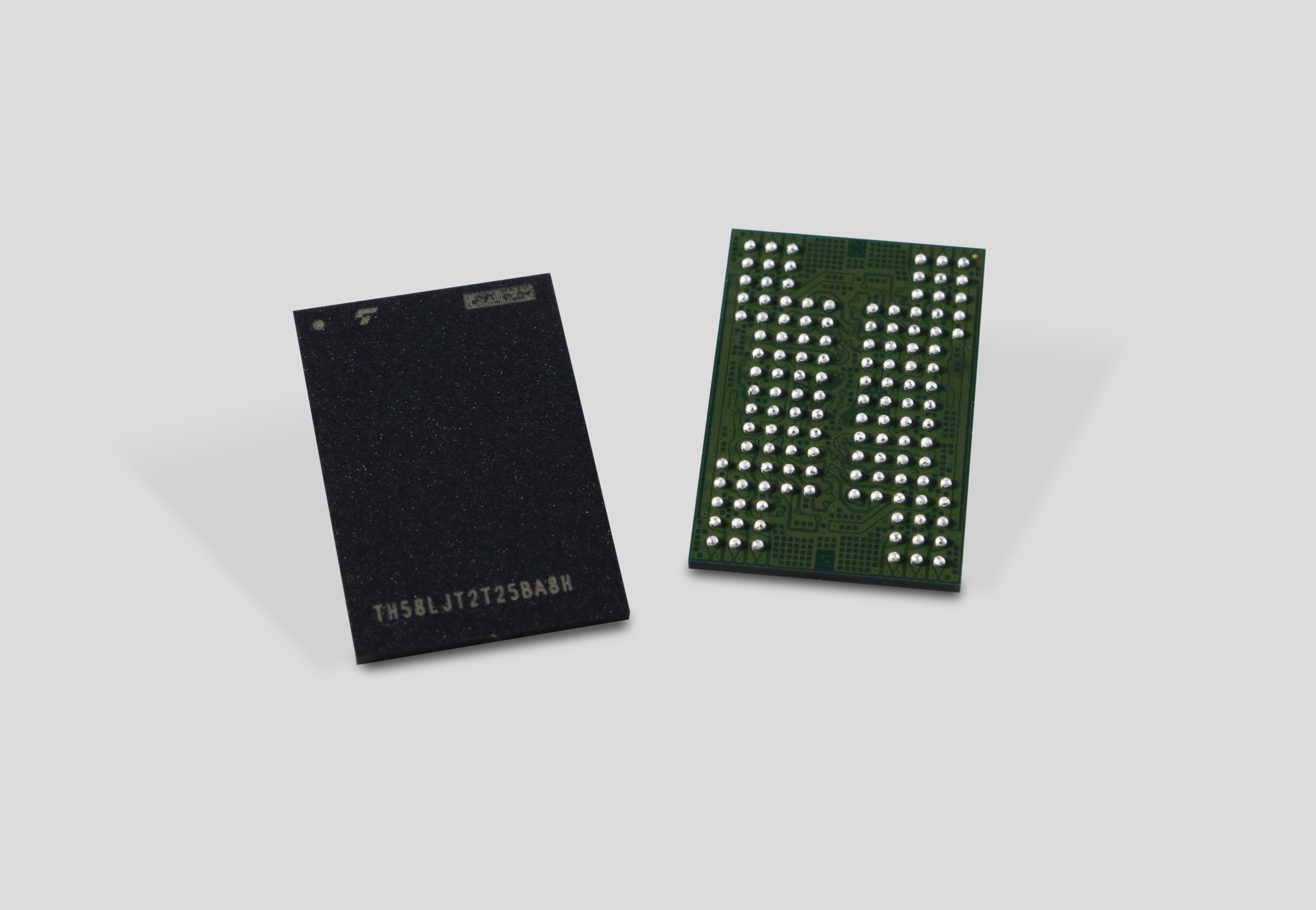
112 layer flash to be sampled in Q1
by David MannersKioxia, the renamed Toshiba, says it will sample a 112-layer TLC flash in Q1. It is the fifth-generation BiCS FLASH 3D flash memory.

The fifth-generation process technology should deliver 1 terabit (128 gigabytes) TLC and 1.33 terabit 4-bit-per-cell (quadruple-level cell, QLC) devices.
The 112-layer stacking process technology increases cell array density by approximately 20% over the 96-layer stacking process.
It also improves interface speed by 50% and offers higher programming performance and shorter read latency.
Fifth-generation BiCS FLASH will be manufactured at the company’s Yokkaichi Plant and the newly built Kitakami Plant.